| Home | Job | Pinball | Photo Album | Automotive | Press/Awards | Contact |

6802/6808 Assembly Code Development
Code Development
One area that I have not previously explored is the development of my own ROMs for the 6802. To get started in this area, I looked into several cross-assemblers, and settled on the A68. One appealing aspect is that it is a small, portable (143 kbytes) DOS command line application. My first goal was to write a small assembly program that demonstrates the basic interactions I would need and then decide later how far to take it. This initial program would 1)read ROM, 2)write and read RAM, and 3)do some PIA output toggling. It would also 4)demonstrate the Reset and Interrupt vectors.
The first thing to figure out is how to set up the code to run. From reading the datasheet on the 6802, the CPU core uses the word at the top of memory as the vector to jump to after a Reset (this is known as the Reset Vector). One important thing to note is that on System 11 (my first target system), the U27 ROM is located starting at address 0x8000. It is a 27256 (a 32kbyte) device. So it spans from CPU address 0x8000 to CPU 0xFFFF. This needs to be taken into account in the constants in the ROM. An example with a super minimal program illustrates this:
; Top of
program
LOOP
ORG $3FFF
JMP $BFFF
; Set up Reset Vector
ORG $7FFE
FCB $BF,$FF
END
Development Environment
I have been using a Dataman S4 for several years to program ROMs, and I know it has an emulator mode. I had initially assumed that I needed to connect the CPU board (the target location) to the ZIF socket where the ROM normally goes, but after emailing the manufacturer, I learned that a special emulator cable plugs into the back of the programmer.
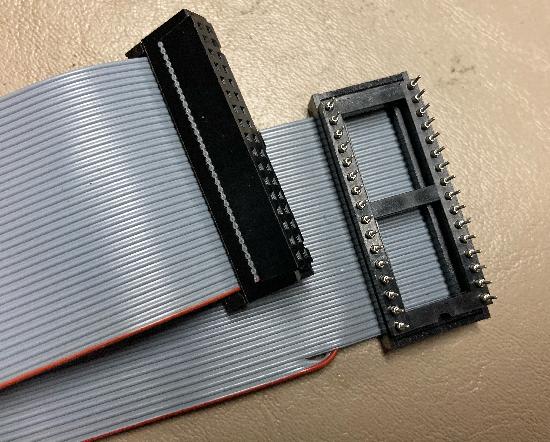
ROM emulation cable for an S4. Left end plugs into the S4,
right end into the target board at the ROM location.
This cable effectively turns the S4 into a ROM chip that can be easily changed and updated via its serial cable. I therefore didn't need to constantly burn and erase ROMs to try code revisions.
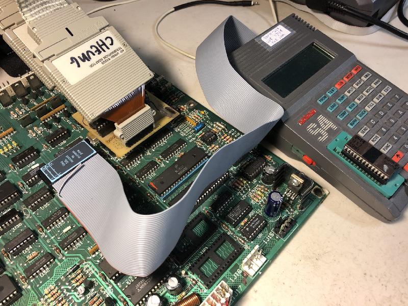
S4 (right) plugged into the System 11 board.
The above images shows the development environment. The S4 is plugged into the System 11 board at the U27 ROM location, and the CPU chip is plugged into a breakout board that allows me to connect in my Logic Analyzer. This latter tool allows me to observe what the CPU chip is doing and do general code debugging.
The power of this setup
is shown by the fact that I can edit the assembly file and
then have that code running on the board in mere seconds.
I can repeat this cycle quickly without having to burn
and UV erase any PROMS. As a note, the hex file that
A68 generates can be transferred directly into the S4
without any processing (set S4 to hex mode).
In Nov 2024, I found out
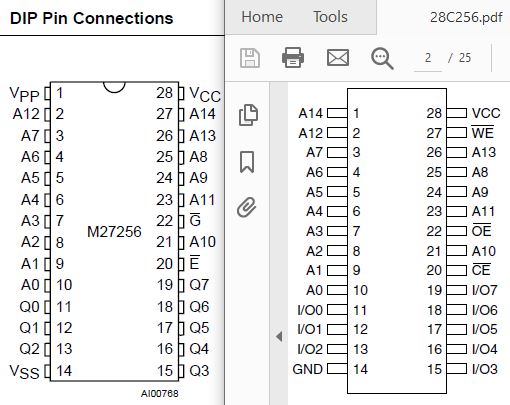
that there is an EEPROM version of the 27256, which is the
28C256. Unfortunately, (to my annoyance) I found out
that the 27C256 and the 28C256 are not exactly pin
compatible. For the latter to be used in a location
for the former, pins 1 and 27 need to be swapped.
Using a web search, I found the above adapter on
Tindie. The DIP switches allow the above pins to be
swapped or not.
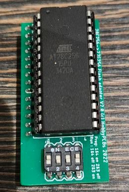
I purchased a few Atmel
28C256 on Amazon for a few dollars each. My Dataman S4
programs these although I do need to change from the
conventional library to the EEPROM one. I suspect
using this vs the emulator would not be quite as fast as I
need to move the part from the programmer to the
board. But it would require less setup than the
emulator.
The sample program (see link below), was assembled and then loaded into the S4 ROM emulator. The Logic Analyzer result is shown on the right side of the image below. This simple program demonstrates most of the goals set above.
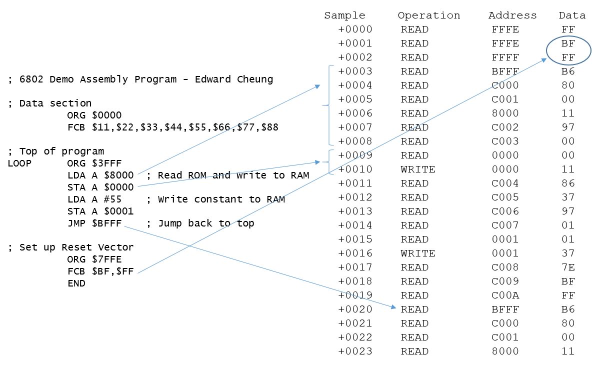
Assembly listing on the left and the Logic Analyzer samples of the Address and Data Bus on the right.
The 'Full' revision below adds understanding of the rest of the interrupt vectors so that the code can be diverted when the test switch on the CPU board is pressed. Future work will be to develop a diagnostic test program like Leon's (RIP), but with some enhancements. It will be available for download in the section below.
Disassembler - Going the other way
One other aspect of assembly development is to be able to possible change or add enhancements to existing code. The first step in this is to decode or reverse the process above and obtain some kind of human readable form from the original binary image. In essense, to dis-assemble the ROM file. After some looking it appears that DASMx is a good choice to check out as it features "code threading". Similar to A86, it runs as a simple, small command line .exe file.
Since I was familiar with it and there were no copyright issues, I ran my 'full' version of the assembly code through it. The first step of that is to obtain a ROM image. The output of the A68 assembler is hex (and can directly be sent into the S4), but DASMx takes a complete binary image. The easiest way for me to obtain that is to read back out the S4 memory. I had previously 'erased' the S4 buffer by filling it with 0xFF, just like an erased ROM would appear. I then created a symbol file so that the Dissassembler could annotate the results accordingly and help me interpret its output. I then ran the program and could see that DASMx correctly interpreted all the bytes as being either instruction or operand. An example is the "Main" loop that loops continuously. A portion of the output is analyzed below.
This is the output from the A68 cross-compiler (assembly to opcode):
;
Top of main to demo read/writes
3000 MAIN ORG $3000 ;@B000 to CPU
3000 b6 80 00 LDA A $8000 ; Read bottom of ROM and write to RAM
3003 97 01 STA A $0001 ; 0001 <- 8000 (memory location)
3005 96 01 LDA A $0001 ; 0001?
3007 86 55 LDA A #$55 ; Write constant to RAM
3009 97 01 STA A $0001 ; 0001 <- 0x55 (literal)
300b 96 01 LDA A $0001 ; 0001?
300d 8e 07 ff LDS #$07FF ; Set location of Stack
3010 7e b0 00 JMP $B000
3000 MAIN ORG $3000 ;@B000 to CPU
3000 b6 80 00 LDA A $8000 ; Read bottom of ROM and write to RAM
3003 97 01 STA A $0001 ; 0001 <- 8000 (memory location)
3005 96 01 LDA A $0001 ; 0001?
3007 86 55 LDA A #$55 ; Write constant to RAM
3009 97 01 STA A $0001 ; 0001 <- 0x55 (literal)
300b 96 01 LDA A $0001 ; 0001?
300d 8e 07 ff LDS #$07FF ; Set location of Stack
3010 7e b0 00 JMP $B000
and this is the listing from the DASMx disassembler (opcode back to assembly):
B000
swi_handler:
B000 rst_handler:
B000 : B6 80 00 ldaa X8000
B003 : 97 01 staa X0001
B005 : 96 01 ldaa X0001
B007 : 86 55 ldaa #$55
B009 : 97 01 staa X0001
B00B : 96 01 ldaa X0001
B00D : 8E 07 FF lds #$07FF
B010 : 7E B0 00 jmp swi_handler
B000 rst_handler:
B000 : B6 80 00 ldaa X8000
B003 : 97 01 staa X0001
B005 : 96 01 ldaa X0001
B007 : 86 55 ldaa #$55
B009 : 97 01 staa X0001
B00B : 96 01 ldaa X0001
B00D : 8E 07 FF lds #$07FF
B010 : 7E B0 00 jmp swi_handler
Note the similarity in the opcodes and the assembly code in both listings. The full listing files are included below.
CPU Board Test ROM - XFlash
Each of the PIAs on the Williams CPU boards have an 8-bit Port A, an 8-bit Port B, and a 4-bit Port C. Unfortunately, Leon's PROM does not test the Port C pins, and I have always wanted to change that. I decided to write my own test PROM as a result. Outputs CA2 and CB2 are not difficult to test, and the new code does that by toggling them. However CA1 and CB1 are input only. They are tested on the board by applying a toggle to these inputs. Once this is done, the code halts toggling of that PIA's outputs to indicate successful reading of the pulse.
On a System 11 board, there are three PIAs that have their CA1 and CB1 pins connected as inputs. The first is U51, the second is U41, and the third is U42. The first one inputs the coin door switches on its CA1 and CB1 pins, so toggling either of those switches will cause the LED2 on the board to stop flashing (that is demonstrated in the video below). The other PIAs have their CA1 and CB1 ports connected to 1J21, so you can test those functions by jumpering to the appropriate pins.
Video of System 11 board running the XFlash ROM.
The above mentioned functions of the test ROM work without using any of the RAM (since this may be faulty in the target CPU board). As a result, I cannot make the use of subroutines as any call would require pushing return information onto the stack. So I had to figure out how to use the CPU's own meager registers to perform tasks such as loops for delays. One such register is the X (index) register. This can be loaded, incremented and tested for a particular value so it makes for a good delay counter. Another available register to use is the Stack Pointer register via 'STS' (Store Stack Pointer). This can be used to stash the Stack into a dummy location and affecting the Condition Code Register, namely the 'Z' flag. As for the other flags, it may be possible to use the Interrupt Enable flag (I) in the Status Register, although if you set it, the IRQ will fire every ~928 instructions (CPU pin 4).
Finally, just like Leon's ROM, pushing the 'test' button on the CPU board will run a RAM test. If that fails, the program will halt and light the LED2 on the CPU board. XFlash is available for download both in assembly and compiled hex code. You just need to burn the code into a 27256 PROM.
Afterwards, I developed the ROM for the System 9 board and got better at assembly. I was able to remove all the absolute jumps and made the code easier to read and more portable. I was then able to combine the System 9 and 11 versions into one file and have a simple IF switch control the assembly process. The source assembly file is available below. To use the hex files, simply download the appropriate one and burn a 27128 ROM for System 9 or a 27256 ROM for System 11.
After further study, I realized that the ROM image for the System 9 would also work for a System 11 if I burned the image in both (top and bottom) halves of the 27256. A test showed this is correct. A single 27256 (with the 2x System 9 image) works in both System 9 and 11 boards. Subsequently I made adjustments to allow the same ROM to run both the main as well as the sound section on both types of boards. So this single ROM can do the work (with improvements) of the four previous versions of Leon's ROMs.
A further update in 2024 accommodates System 3-7 by moving all code into the top 0x800 of ROM, and adding any PIAs that were missing from before. A compiler switch handles any shifting of the memory ranges that is needed.
68B09 Code Development
Williams switched to the 6809 for the WPC series of boards (the 68B09 is the higher speed version). Unfortunately, it does not use the same instruction set and when I decided to develop code for this processor I needed to find an assembler for it. There appear to be two common options. AS9 is the original assembler developed by Motorola. Unfortunately, I could not build an executable from the source C files, and the .exe file did not run on my 64 bit machine. Fortunately asm6809 did work for me. Besides the assembler, one nice tool I discovered is an online 6809 emulator. It allows you to run code that you develop in a convenient setting.
Here is a sample of 6809 assembly code (see link to Demo.asm below).
org $F000 ; Put main near top of ROMThe code assembles to a small .hex file and that is easily copied to my S4 programmer. I do have to 'move' the code from top of CPU address space (0-0x0FFFF) to top of PROM (0-0x1FFFF).
main nop
lda #$55
sta $0400 ; write RAM
lda #$7A
sta $0401 ; write RAM
lda $0400 ; read RAM
lda $0401 ; read RAM
nop
jmp main ; Loop
Instead of tediously UV erasing 27C010 (1 Megabit) PROMs, I decided to try and use the 28C256 EEPROM for quick code development. As long as the total program space is 0x8000 (32 kBytes) or less, it will fit and run. To do this, the code needs to be moved from 0xF000-0xFFFF to 0x7000-0x7FFF. This is the top of the 27256 PROM (same as 28C256). The second mod is to connect pin 28 of the PROM to pin 32 of the 27C010 socket. This can be done by modifying a 32 pin IC socket as shown below.

View of the underside of the 27256 adapter. Top most pin here
is pin 32 of the 27C010, which is the Vcc pin. With a small wire,
solder that to the bent pin 30 of the socket. Once inserted,
this pin will not plug into the WPC board.

View of the WPC board with the adapter socket. Once the
above modified socket is plugged into U6 of the WPC board,
it will accept a 27C256 or an adapted 28C256.
Note that the ASIC maps the 1 Megabit
27C010 PROM to pages for the 68B09 CPU. But the top
half of the CPUs address space is not paged.
Addressing 0x8000 to 0xFFFF will always retrieve the top
0x8000 of the 1 Megabit PROM. By using the adapter
above, Address lines A16 and A15 are ignored, and maps the
contents of the 27256 to CPU 0x8000-0xFFFF. This is
important as the Reset Vector of the 68B09 is at 0xFFFE
and 0xFFFF.
- March 2021. Start of work with assembler.
- October 2021. Replaced the 7 AA rechargeable batteries inside the S4 Dataman. I had previously added a trickle charge feature, and that was helpful in keeping the batteries charged. However, by this date, two batteries had failed and I decided to replace the pack with 7 NiMH batteries. The originals were assembled in Sept 1997, so they lasted 24 years.
- November 2022. Added more checks of RAM and inverted Port C polarity (on all PIAs) to cause flipper relay to click. These were requests from Clay Harrell.
- November 2024. Rev 1.4. Modified for System 3-7 by moving all code into top 0x800 of ROM so it fits into a 2716. This is doubled for a 2532/2732 (System 7). RAM check also adjusted for size.
- April 2025. Development of 6809 code.
Links
- My main Pinball CPU repair page
- A68 Cross Compiler
- DASMx
Disassembler (version 1.4 - 2003)
- Leon Borre's test ROM
- Alternate test
ROM (German origin)
- Assembler files I wrote
- Basic program (Feb 2021)
- Full program (March 2021 - completes numbered objectives above)
- Logic Analyzer
capture of the above run on a System 11 board.
- Listing file generated by A68.
- Listing file generated by DASMx based on the binary image.
- Symbol file for DASMx.
- XFlash Test ROM program (version 1.1) runs on both 9 and 11.
- Binary image for 27256.
- Demo.asm
for 6809
- Rev
1.4 that supports all Williams (using assembler
switch).
- Tutorials on assembly. Learning to program the 6802
- Manual on the registers and instruction set (author unknown).
- Programming book by W. Sirichote.
- Nano - The small 6802 Single Board Computer
(c) 2024 Edward Cheung, all rights reserved.