| Home | Job | Pinball | Photo Album | Automotive | Press/Awards | Contact |

WPC DCS Sound and CPU FPGA Project (Page 2)
See here for Page 1These include the two ASICs and PAL.
Bypassing
the security PIC
WPC-S and WPC-95 CPU boards contain a programmed Microchip PIC processor which functions as a serial number key. My next task was to find a way to incorporate that function also in my FPGA. This would lead to a universal WPC CPU board, potentially able to handle the various generations of WPC in one board.
Bypassing - Approach 1.
The first approach was to simply emulate the PIC inside the FPGA. I had a lot of assistance from Martin, who sent me a fact file written by the developer of WPCMame, and Brent, who developed an aftermarket Security PIC. Essentially, the PIC contains 16 data bytes that has a serial number encoded into it. The bytes are read in a random order, and two of these bytes rotate in value every time a byte is read. This randomization and rotation is meant to make it difficult to reverse engineer the PIC. My hat is off to the developer of WPCMame who reverse engineered the algorithm (as far as I know). It is very complex.
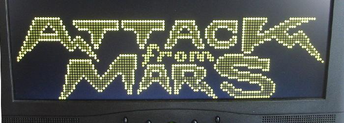
The screenfuls below show the successful emulation of a Medieval Madness Security PIC. I used the VGA display for convenience. The top screen shows the startup screen. One can see the "50059" and the "559", which represent the game number for Medieval Madness in two formats (one with the "00" coin door code, and one without). The rest of the bottom line is the serial number. I used the same format as the aftermarket Security PIC.


Two screenfuls on my VGA display that show the successful emulation of the
Security PIC. The top screen is the WPC-S boot up message. "559" is the
game number (MM), and the rest is the serial number for this particular
machine. Note that the two-tone shading of the pixels is correctly
emulated on the VGA display.
WPC-S and WPC-95 CPU boards contain a programmed Microchip PIC processor which functions as a serial number key. My next task was to find a way to incorporate that function also in my FPGA. This would lead to a universal WPC CPU board, potentially able to handle the various generations of WPC in one board.
Bypassing - Approach 1.
The first approach was to simply emulate the PIC inside the FPGA. I had a lot of assistance from Martin, who sent me a fact file written by the developer of WPCMame, and Brent, who developed an aftermarket Security PIC. Essentially, the PIC contains 16 data bytes that has a serial number encoded into it. The bytes are read in a random order, and two of these bytes rotate in value every time a byte is read. This randomization and rotation is meant to make it difficult to reverse engineer the PIC. My hat is off to the developer of WPCMame who reverse engineered the algorithm (as far as I know). It is very complex.
The screenfuls below show the successful emulation of a Medieval Madness Security PIC. I used the VGA display for convenience. The top screen shows the startup screen. One can see the "50059" and the "559", which represent the game number for Medieval Madness in two formats (one with the "00" coin door code, and one without). The rest of the bottom line is the serial number. I used the same format as the aftermarket Security PIC.
Two screenfuls on my VGA display that show the successful emulation of the
Security PIC. The top screen is the WPC-S boot up message. "559" is the
game number (MM), and the rest is the serial number for this particular
machine. Note that the two-tone shading of the pixels is correctly
emulated on the VGA display.
The concept of how this
approach would be used is to modify the game code with "ANYPIC.EXE".
This
x86
program,
from the developer of WPCmame, takes the original game code, and
modifies it to allow the use of any valid
Security PIC. With this modification to the game code,
potentially any WPC ROM can be run. I successfully tested
with Slug Fest (WPC-DMD), Indiana Jones (WPC-DCS), and Medievel Madness
(WPC-95) using the same FPGA image.
Bypassing - Approach 2.
I wanted to create a system by which any original Williams ROM could be run without modification, and also without setting a bunch of jumpers on the FPGA to indicate which ROM is in use. This required the bypassing of the Security PIC check. An algorithm on how to do this was developed by WPCmame in 2000, but I did not understand his write-up. Looking at several ROMs, his algorithm did not match with the contents of the ROMs. I set off on developing my own way, and here Chip Scope was a big help. I was able to see the ROM code read the PIC's security string, and the reading of the game ID. After lots of tracing, I realized the discrepancy from WPCmame's document, and could make sense of it.
Essentially, the Spartan VHDL code does the following to bypass the Security PIC check:
- When the system reset is released, the FPGA takes control of the ROM address bus and holds the CPU in reset.
- The ROM is searched sequentially for "EC 9F xx yy 83 12 34". This is a pattern that marks the address of a pointer to the location of the game ID. This search takes only a few tens of milliseconds.
- The ROM address bus is then released and then turned over
to the CPU. Its reset is then released allowing the WPC board
to boot up normally.
- When the CPU asks for the game ID (at the previously determined location), the game ID for Medieval Madness is substituted.
- Combined with the emulation of the Security PIC previously described, it causes the ROM code to pass the PIC check regardless of the original ROM contents.
This algorithm was coded
up and testing was successful. So far, I have tested with MM
v1.0, AFM v1.0, and TOTAN v1.4. They all pass the Security
PIC test successfully and run their attract mode animation.
One note I would like to mention is that the Spartan board has 4 Mbyte
of Flash. Each image of a WPC ROM code is 512K bytes (or 256K
for early WPC). By using three slide switches on the board,
I can have up to eight game code ROMs loaded into
Flash. For example, as of this writing, I can switch between
Slug Fest, IJ, MM, AFM, and TOTAN by simply sliding the switches, and
hitting the reset button. It is incredibly cool to see a
small Spartan board with a VGA monitor plugged into it run WPC code as
if it were inside a large pinball machine.
This shows the VGA display with AFM ROMs being used.
One additional
interesting aspect is that this new PIC bypass mode does not seem to
interfere with non Security ROMs. Running this preboot check
still allows older code to run just fine. So far testing has
only included IJ and Slug Fest, but in case of problems, the check can
be disabled by using a jumper on the board.

The DMD/VGA interface with the Real-Time Clock added into the WPC prototype.
It took several days to make sure that the day counter was tracking properly, but I decided to call it a success at the date and time above. I now no longer receive the "Factory Settings Restored" message on power up, showing that the NV RAM function was working. Of course, the CPU LED still gave me the fast flashing on startup to indicate all the checksums operated correctly.
Development Tools
As in many endeavours, having the right tools will make the task easier. Here are the main tools that I developed for the WPC FPGA project.
I realized that I would need to use a Logic Analyzer on an actual WPC machine one day. The picture below shows how it was normally connected to the CPU board via a "rat's nest" of probes. It would obviously be very difficult to use this setup on a real pinball machine. I decided to make an adapter board for the 20-pin isolation adapter probes for the HP Logic Analyzer.

The reference WPC CPU and DMD board connected to my Logic Analyzer. What a mess of wires!
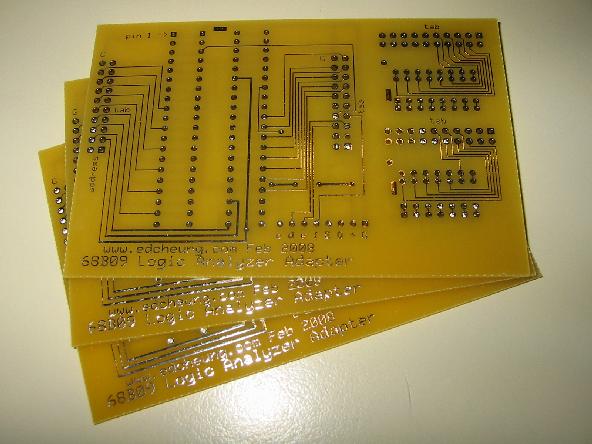
I decided to make an adapter daughter board that would allow direct plug-in of the Logic Analyzer.
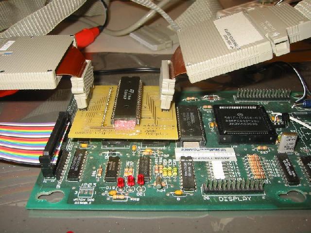
Plug-in board in use. No more rat's nest.
Dev Tools 2: Using a real CPU chip
Where
we stand at this point
So to summarize, the Spartan FPGA that emulates a CPU board contains the following functionality:
Too
much time on my hands : Interfacing to a real-time clock
The original WPC CPU board has three AA batteries to preserve RAM contents and to power the real-time clock (RTC) that is inside the ASIC. I looked for a chip that would do both functions in one package. I considered selections from a number of vendors, but quickly settled on Maxim due to their strong overall product line. They had acquired Dallas Semiconductor a number of years ago, which made their RTC line very strong. In our application, we need a hour:minute clock with a binary (not BCD) output, and a five-bit day-of-year counter. We also need at least 4k bytes of Non-Volatile (NV) storage. I also preferred this later function to be direct (non multiplexed) interface. This would allow the CPU to access the RAM directly, instead of needing to load a separate address register for each access.
After some searching it became apparent that there was no chip available that could do exactly what I wanted. The closest is the DS1744/DS1743 (and similar) series. This chip offers BCD output instead of binary. This means that, for example, the number '12' (decimal twelve) is represented by two nibbles. The first will have the value "0x1", and the second "0x2". Thus this number will represented by "0x12" instead of "0x0C". I wrote some conversion routines in VHDL to convert from binary to BCD (for setting the time), and from BCD to binary (for reading the time). I also added functions to convert the calendar day and month to a day-of-year function.

The DS1744 plugged into the solderless breadboard and connected to the Spartan.
One nice aspect of dealing with Maxim is their policy of sending you free samples of their chips. I was able to receive several DS1744 for no charge. These retail for about $25 in single quantities at Digikey. Interfacing the RAM functions to the Spartan was straightforward (due to the non-multiplexed bus), but the time functions took some more work.
The original WPC CPU board has three AA batteries to preserve RAM contents and to power the real-time clock (RTC) that is inside the ASIC. I looked for a chip that would do both functions in one package. I considered selections from a number of vendors, but quickly settled on Maxim due to their strong overall product line. They had acquired Dallas Semiconductor a number of years ago, which made their RTC line very strong. In our application, we need a hour:minute clock with a binary (not BCD) output, and a five-bit day-of-year counter. We also need at least 4k bytes of Non-Volatile (NV) storage. I also preferred this later function to be direct (non multiplexed) interface. This would allow the CPU to access the RAM directly, instead of needing to load a separate address register for each access.
After some searching it became apparent that there was no chip available that could do exactly what I wanted. The closest is the DS1744/DS1743 (and similar) series. This chip offers BCD output instead of binary. This means that, for example, the number '12' (decimal twelve) is represented by two nibbles. The first will have the value "0x1", and the second "0x2". Thus this number will represented by "0x12" instead of "0x0C". I wrote some conversion routines in VHDL to convert from binary to BCD (for setting the time), and from BCD to binary (for reading the time). I also added functions to convert the calendar day and month to a day-of-year function.
The DS1744 plugged into the solderless breadboard and connected to the Spartan.
One nice aspect of dealing with Maxim is their policy of sending you free samples of their chips. I was able to receive several DS1744 for no charge. These retail for about $25 in single quantities at Digikey. Interfacing the RAM functions to the Spartan was straightforward (due to the non-multiplexed bus), but the time functions took some more work.
The DMD/VGA interface with the Real-Time Clock added into the WPC prototype.
It took several days to make sure that the day counter was tracking properly, but I decided to call it a success at the date and time above. I now no longer receive the "Factory Settings Restored" message on power up, showing that the NV RAM function was working. Of course, the CPU LED still gave me the fast flashing on startup to indicate all the checksums operated correctly.
Development Tools
As in many endeavours, having the right tools will make the task easier. Here are the main tools that I developed for the WPC FPGA project.
I realized that I would need to use a Logic Analyzer on an actual WPC machine one day. The picture below shows how it was normally connected to the CPU board via a "rat's nest" of probes. It would obviously be very difficult to use this setup on a real pinball machine. I decided to make an adapter board for the 20-pin isolation adapter probes for the HP Logic Analyzer.
The reference WPC CPU and DMD board connected to my Logic Analyzer. What a mess of wires!
I decided to make an adapter daughter board that would allow direct plug-in of the Logic Analyzer.
Plug-in board in use. No more rat's nest.
The above daughter board
allows access to all of the CPU's pins. This includes the
address, and data bus, as well as all the control lines and
clocks. This board allows me to use the "01650-63203"
isolation adapter for HP scopes (archived).
Dev Tools 2: Using a real CPU chip
There are times when I
want to verify that the VHDL CPU core that I am using is
correct. I do this by plugging in a solderless breadboard to
the Spartan, which has an original 68B09 CPU chip mounted into
it. I have a special project prepared that then moves the
functionality of the CPU from the internal VHDL core to the physical
chip on the outside. This has shown me that the 68B09 core
that I use is running accurately and correctly.

This solderless breadboard has an real 68B09 CPU chip for comparing results with the VHDL CPU core.
There is also the case when I need to run my system with a real ASIC
and board to see how it behaves. One way is to use the above
setup, and jumpering the 40 pins of the CPU pins into the corresponding
ones on the WPC board. Along with a project file specific to
this configuration, I can use a real ASIC with the VHDL CPU core, or I
can run both ASICs simultaneously to see the difference between my
simulated ASIC and the real one.
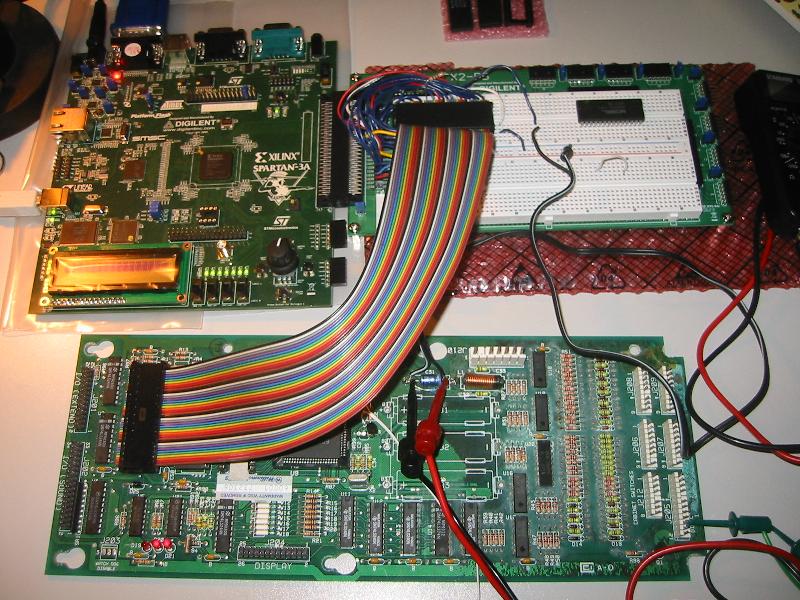
With this setup, I can run my Spartan code with a real WPC ASIC.
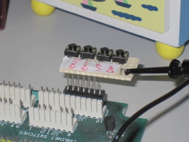
DevTools 4: Coin Door Switches
This little attachment is all I need to navigate through the DMD menu.
The test point allows access to board ground to hit other switches.
Another sidebar: Repair of the HP 1652B Power Supply.
This solderless breadboard has an real 68B09 CPU chip for comparing results with the VHDL CPU core.
Dev
Tools 3: Using a real WPC ASIC and board
With this setup, I can run my Spartan code with a real WPC ASIC.
DevTools 4: Coin Door Switches
Now that I can see the
DMD display on my VGA screen, I needed a way to navigate the
menus. I decided that a small plug-in board with some
switches was the right compact way to access these features.
I also add a small test point to access the board ground.
This way I can use my mini-grabber probe to ground the other switches.
This little attachment is all I need to navigate through the DMD menu.
The test point allows access to board ground to hit other switches.
Another sidebar: Repair of the HP 1652B Power Supply.
So to summarize, the Spartan FPGA that emulates a CPU board contains the following functionality:
- 6809 CPU
- CPU board RAM
- CPU board ASIC
- Security PIC
- DMD & VGA interface
- State machine to interface to Real-Time Clock and
Non-Volatile RAM
- Minor glue logic chips from the CPU board.
- Chip Scope debugging core.
The part on the Spartan
3A board is an XC3S700A
(700k gates). Utilization of the Spartan's
Flip-Flops stands at around 33%, and needs an 'equivalent gate count'
of 50,000 gates. The utilization of the RAM is unknown due to
the inclusion of the Chips Scope core, which takes up all available
RAM. Considering only flip-flop utilization, the design above
will fit into an XC3S200AN.
In
single
quantities,
these
cost about $25 in single quantities at Digikey. If a full
'700 is needed, these cost about $60 in singles.
Acknowledgment
The following have contributed to this project. I am very grateful for their assistance.
John Kent - For his CPU VHDL core and his patient answering of many e-mails.
Martin Reynolds - For his constant assistance with ideas and his knowledge of PinMAMED.
Brent Butler - Who provided the PAL equations and assisted with the Security PIC.
Martin Adrian (aka WPCmame) - for the IO map of the CPU ASIC & Security PIC algorithm.
John Wart Jr. - Who loaned me a WPC-DCS board.
Jim Knight - Who loaned me a WPC-95 A/V board.
If you are interested in assisting with this project, please send me e-mail.
I am looking for an IP core for the A/V DSP.
Go to Page 3 of this project
- Continued from Page
1.
- 2/17/08 - Successful emulation of the Security PIC inside the FPGA.
- 2/20/08 - Successful bypass of the PIC. Now any WPC ROM can be run on the Spartan without modifications.
- 2/29/08 - Logic Analyzer adapter
for the 68B09 CPU chip, and other development tools.
- 3/9/08 - Found bug in my SHIFTEDBIT section that caused the switch matrix to not be scanned properly. Scanning of matrix and diagnostic buttons now work.
- 3/11/08 - Figured out with Brent's cooperation how to handle the zero crossing information for GI dimming, and TRIAC control.
- 3/13/08 - The format of the two HOUR and MINUTE registers in the ASIC is now clear. There is also a five-bit field for DAY. If my theory is correct, it means that if a WPC machine is not powered up every 31 days, it will lose track of the date. Discussed here.
- 3/25/08 - Interface to Maxim DS1744 Real-Time Clock and NV RAM works.
- Go to Page 3.
(c) 2012 Edward Cheung, all rights reserved.