| Home | Job | Pinball | Photo Album | Automotive | Press/Awards | Contact |

WPC DCS Sound and CPU FPGA Project (Page 1)
Using an FPGA to
replicate no longer available components on the
Sound and CPU Boards in a WPC-DCS Pinball Machine.
These include the two ASICs and PAL.
Sound and CPU Boards in a WPC-DCS Pinball Machine.
These include the two ASICs and PAL.
Introduction
With the introduction of Indiana Jones in 1993, Williams Pinball started to base their audio system on the Digital Compression System. The main CPU for this system is an ADSP-2105 DSP chip. There were two main generations of these boards, the first (used in the IJ) used a PAL to contain the decoding logic. This is known as the WPC-DCS audio board. In the second generation, Williams combined the dot matrix controller onto the same board, and moved all the logic into an ASIC. This latter generation is known as WPC-95.
Due to the unavailability of the ASIC, the WPC-95 audio boards have soared in price (RGP discussion). They are commonly several hundred dollars each. In the summer of 2007, I was looking for a pinball/FPGA related project, and this seemed like a good one to dive into. After some discussion with Martin Reynolds, I decided to give it a try.
The first step was to reproduce the WPC-DCS circuit, since it was simpler (only uses a PAL). My hope was that once it was running using IJ ROMs, I could make some small changes, load in MM ROMs, and show that WPC-95 was simply a repackaging of WPC-DCS. To get started, I needed to know the equations for U16, the PAL on the WPC-DCS board. Help came from Brent Butler, who was the one who reverse engineered the WPC Security PIC. He read the contents of his PAL, and sent me the equations. This, along with the WPC-DCS schematics, and the part datasheets were all the ingredients I needed to start coding.
The prototype/breadboard
The platform I chose to use was the Spartan3A development board. It includes a Spartan3A FPGA, and lots of peripherals such as 4 MBytes of Flash, buttons, LEDs, a power supply, a USB programmer, and an expansion connector. This latter connector allowed the connection to wire wrap boards, where the DSP and D/A chips would reside. The self-contained Flash memory was nice because it would allow me to eliminate the large PROM chips, and put their contents in a compact modern part. IJ needs 3.5 MBytes, so it should fit quite nicely.
The first step was to load the ROMs for the IJ into the Flash of the Spartan3A board. The image of the seven sound ROMs were merged into one large binary file, and I then used Ken Chapman's excellent Flash loader (see link below) to transfer this into the Spartan 3A. Once that was complete, I could use his bootloader program to read back sections, and I could see that the 7 chip image was correctly loaded into the Flash. The next step was to develop the VHDL code. A simulation of the result is shown below.

In the above waveform diagram, the signals from 'cmd_read' to 'ram_read' indicate what the decoding logic thinks the DSP is doing. We can see only one of these become asserted at any one time. Also, an inspection of the databus shows the proper data being fetched for the DSP. This shows that the PAL equations and my reading of the schematic appear to be correct.
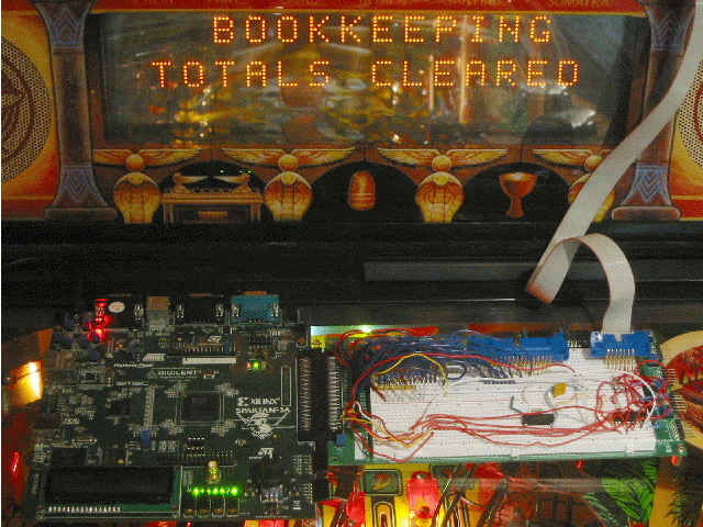
Once the code was complete, it came time to assemble the prototype. As mentioned before, the DSP and D/A were to be installed onto the breadboard that plugs into the Spartan3A. I decided to mount them pin side up to allow access to all the connections. A photograph of the completed prototype is shown below.
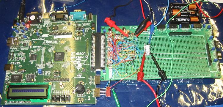
The WPC-DCS prototype board. The board on the right holds the DSP and the D/A.
All other components are on the other board.
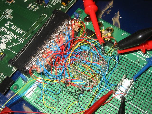
Close-up of the DSP and D/A area. The two components are on the reverse side.
The DSP is mounted into a socket, and then plugged into some wire wrap pins. This is the square grid of pins in the above image. To the right of that is the 16-pin D/A chip, also mounted pin side up. The D/A needs a -5V supply, and this is supplied by a AA battery pack. As you can see in the image above, the DSP connects to the Spartan via series resistors. These are included to protect the Spartan 3 device because its inputs are not 5V tolerant.
Testing
I did some tests to characterize what the DSP is supposed to do on startup. When an original WPC-DCS board is properly running, the clock (DacClk) and strobe (DacStb) lines from the DSP to the D/A are expected to be clocking, but the data (DacDat) line will be static. The data line will have transitions only when a sound is being played. Also, the power-up BONG is expected to be played by the DSP a few seconds after bootup. In contrast, a WPC-DCS board with no ROMs installed, will have these lines as hi-Z, which is presumably the power-on state for this port. Clearly, there will be no sound issued by the DSP if it does not boot. This information will allow me to gauge if the DSP on the prototype is running or not.
Up to this point, a lot of effort had been invested, and if the DSP did not boot, I would have very few options to incrementally debug the problem. A great deal was at stake here, and it would all hinge on the initial power-up. I flipped the power switch, and to my relief, the DSP appeared to be working. I could see the D/A lines clocking, and a single burst would appear on the data line a few seconds after power-up. Also, I programmed the switches on the Spartan 3A for command input (to play sounds), and when a command was sent to the DSP, I could see it fetch the command, and clear the interrupt flag. This was very promising.
I then plugged in the D/A chip next. In addition to the usual 5V, this chip requires -5V as well. Presumably for the internal audio op amp. This latter supply is provided by a battery pack. I connected the audio output of this chip to a signal tracer (basically a small audio amplifier with speaker). On the subsequent power up, I get a cool single "BONG" from the prototype. This indicates the DSP boots and that the checksum of all the Flash was good. Success!
The DCS audio board is controlled by a bus consisting of 8 data bits, 5 address bits, and 2 control lines. I needed to know what commands the DSP code would recognize so that I can stimulate it on my test bench. Help came once again from Martin, who knows how to run PinMAMED. Using this emulator/debugger, we were able to figure out that command packets are two bytes long. For example "0001" causes the Indy march to play on PinMAMED. A check with an oscilloscope on my IJ shows that the two bytes are normally separated by about 1 millisecond. Based on my initial testing with sending single bytes, the DSP times out after a certain period, and the two bytes in the packet need to follow each other by 1 millisecond or less. I then changed my user interface to send two bytes in rapid succession, with the bottom nibble controlled by the four slide switches on the Spartan3A board. This proved successful, and I was able to get my prototype to play all the sounds identified by 0001 through 000F on PinMAMED.
WPC-95
The next step was to emulate/replicate the WPC-95 A/V board. When this project was started, I had hoped to be able to simply port the WPC-95 ROMs into the testbed above. This would eliminate my having to reverse engineer the ASIC. However, examination of the schematic shows why this would not work.
With the introduction of Indiana Jones in 1993, Williams Pinball started to base their audio system on the Digital Compression System. The main CPU for this system is an ADSP-2105 DSP chip. There were two main generations of these boards, the first (used in the IJ) used a PAL to contain the decoding logic. This is known as the WPC-DCS audio board. In the second generation, Williams combined the dot matrix controller onto the same board, and moved all the logic into an ASIC. This latter generation is known as WPC-95.
Due to the unavailability of the ASIC, the WPC-95 audio boards have soared in price (RGP discussion). They are commonly several hundred dollars each. In the summer of 2007, I was looking for a pinball/FPGA related project, and this seemed like a good one to dive into. After some discussion with Martin Reynolds, I decided to give it a try.
The first step was to reproduce the WPC-DCS circuit, since it was simpler (only uses a PAL). My hope was that once it was running using IJ ROMs, I could make some small changes, load in MM ROMs, and show that WPC-95 was simply a repackaging of WPC-DCS. To get started, I needed to know the equations for U16, the PAL on the WPC-DCS board. Help came from Brent Butler, who was the one who reverse engineered the WPC Security PIC. He read the contents of his PAL, and sent me the equations. This, along with the WPC-DCS schematics, and the part datasheets were all the ingredients I needed to start coding.
The prototype/breadboard
The platform I chose to use was the Spartan3A development board. It includes a Spartan3A FPGA, and lots of peripherals such as 4 MBytes of Flash, buttons, LEDs, a power supply, a USB programmer, and an expansion connector. This latter connector allowed the connection to wire wrap boards, where the DSP and D/A chips would reside. The self-contained Flash memory was nice because it would allow me to eliminate the large PROM chips, and put their contents in a compact modern part. IJ needs 3.5 MBytes, so it should fit quite nicely.
The first step was to load the ROMs for the IJ into the Flash of the Spartan3A board. The image of the seven sound ROMs were merged into one large binary file, and I then used Ken Chapman's excellent Flash loader (see link below) to transfer this into the Spartan 3A. Once that was complete, I could use his bootloader program to read back sections, and I could see that the 7 chip image was correctly loaded into the Flash. The next step was to develop the VHDL code. A simulation of the result is shown below.
Simulation of the VHDL
code shows no bus contention and the proper data
being fetched for the DSP. In general, the signal names are the same as
on the WPC-DCS schematic.
being fetched for the DSP. In general, the signal names are the same as
on the WPC-DCS schematic.
In the above waveform diagram, the signals from 'cmd_read' to 'ram_read' indicate what the decoding logic thinks the DSP is doing. We can see only one of these become asserted at any one time. Also, an inspection of the databus shows the proper data being fetched for the DSP. This shows that the PAL equations and my reading of the schematic appear to be correct.
Once the code was complete, it came time to assemble the prototype. As mentioned before, the DSP and D/A were to be installed onto the breadboard that plugs into the Spartan3A. I decided to mount them pin side up to allow access to all the connections. A photograph of the completed prototype is shown below.
The WPC-DCS prototype board. The board on the right holds the DSP and the D/A.
All other components are on the other board.
Close-up of the DSP and D/A area. The two components are on the reverse side.
The DSP is mounted into a socket, and then plugged into some wire wrap pins. This is the square grid of pins in the above image. To the right of that is the 16-pin D/A chip, also mounted pin side up. The D/A needs a -5V supply, and this is supplied by a AA battery pack. As you can see in the image above, the DSP connects to the Spartan via series resistors. These are included to protect the Spartan 3 device because its inputs are not 5V tolerant.
Testing
I did some tests to characterize what the DSP is supposed to do on startup. When an original WPC-DCS board is properly running, the clock (DacClk) and strobe (DacStb) lines from the DSP to the D/A are expected to be clocking, but the data (DacDat) line will be static. The data line will have transitions only when a sound is being played. Also, the power-up BONG is expected to be played by the DSP a few seconds after bootup. In contrast, a WPC-DCS board with no ROMs installed, will have these lines as hi-Z, which is presumably the power-on state for this port. Clearly, there will be no sound issued by the DSP if it does not boot. This information will allow me to gauge if the DSP on the prototype is running or not.
Up to this point, a lot of effort had been invested, and if the DSP did not boot, I would have very few options to incrementally debug the problem. A great deal was at stake here, and it would all hinge on the initial power-up. I flipped the power switch, and to my relief, the DSP appeared to be working. I could see the D/A lines clocking, and a single burst would appear on the data line a few seconds after power-up. Also, I programmed the switches on the Spartan 3A for command input (to play sounds), and when a command was sent to the DSP, I could see it fetch the command, and clear the interrupt flag. This was very promising.
I then plugged in the D/A chip next. In addition to the usual 5V, this chip requires -5V as well. Presumably for the internal audio op amp. This latter supply is provided by a battery pack. I connected the audio output of this chip to a signal tracer (basically a small audio amplifier with speaker). On the subsequent power up, I get a cool single "BONG" from the prototype. This indicates the DSP boots and that the checksum of all the Flash was good. Success!
The DCS audio board is controlled by a bus consisting of 8 data bits, 5 address bits, and 2 control lines. I needed to know what commands the DSP code would recognize so that I can stimulate it on my test bench. Help came once again from Martin, who knows how to run PinMAMED. Using this emulator/debugger, we were able to figure out that command packets are two bytes long. For example "0001" causes the Indy march to play on PinMAMED. A check with an oscilloscope on my IJ shows that the two bytes are normally separated by about 1 millisecond. Based on my initial testing with sending single bytes, the DSP times out after a certain period, and the two bytes in the packet need to follow each other by 1 millisecond or less. I then changed my user interface to send two bytes in rapid succession, with the bottom nibble controlled by the four slide switches on the Spartan3A board. This proved successful, and I was able to get my prototype to play all the sounds identified by 0001 through 000F on PinMAMED.
A short video of
the board playing the Indy march.
WPC-95
The next step was to emulate/replicate the WPC-95 A/V board. When this project was started, I had hoped to be able to simply port the WPC-95 ROMs into the testbed above. This would eliminate my having to reverse engineer the ASIC. However, examination of the schematic shows why this would not work.
- WPC-95 ROMs are larger than WPC-DCS. Per the
schematic, the
address bus for the WPC-DCS ROMs is 23 bits wide (8 Mbytes address
space). In contrast, the address bus on WPC-95 is 24 bits (16
Mbytes address space).
- Of this latter 24 bits, the 10 LSB bits come directly from the DSP address bus, while the remaining 14 come from a paging register inside the ASIC. This is much different than WPC-DCS, where the bottom 12 bits are from the DSP, and the top 11 from a paging register.
- Only 8 bits of the DSP's data bus is connected to the ASIC, thus the 14 bits of the paging register must be stored as two separate writes. This makes the two platforms incompatible. Loading the paging register is completely different in one configuration compared to the other.
- There are two RAM enable signals on WPC-95 (both from ASIC) vs. one on the WPC-DCS.
Cracking
the code
An important tool to understand what the ASIC and DSP are doing is a logic analyzer. I connected three pods of my unit to the various points on the WPC-95 board that was loaned from Jim Knight. This unit had Scared Stiff ROMs on it. I was able to slowly gain an understanding of what the DSP does using this setup. It felt like the process of cracking a cipher code or opening a combination lock.

The logic analyzer connected to a WPC-95 board.
The order of operations of the DSP is as follows:
An important tool to understand what the ASIC and DSP are doing is a logic analyzer. I connected three pods of my unit to the various points on the WPC-95 board that was loaned from Jim Knight. This unit had Scared Stiff ROMs on it. I was able to slowly gain an understanding of what the DSP does using this setup. It felt like the process of cracking a cipher code or opening a combination lock.
The logic analyzer connected to a WPC-95 board.
The order of operations of the DSP is as follows:
- When the POR timer expires, the DSP reads the inital boot code from ROM using the BMS signal. This takes about 610 useconds.
- The internal boot functions take about 300 useconds, and the first of the RAM checks then start.
- A pattern is written to the entire range of RAM using the DMS line.
- The pattern is read back using the DMS line.
- Another pattern is written to RAM with the PMS line.
- The pattern is read back using the PMS line.
- If any of the previous four steps fail, the DSP issues ten
bongs. This checkout takes about 200 microseconds.
- RAM is then erased with the PMS line.
- Another erasure of RAM with the DMS line.
- The DSP then proceeds to the checksum calculation of the ROMs. This takes about 2 seconds on Scared Stiff ROMs.
- If all is well, at t=2.5 seconds, the BONG starts. A single sound indicates all is well with the ROMs. This takes about 0.6 seconds.
- At t=3.4 seconds, the DSP reads from ROMs again with the BMS line. At this point, the DSP starts to operate.
- While this is going on, every second or so, the DSP writes
to a
register in the ASIC to flash the red LED on the board on and off.
Another important tool
is Xilinx's
Chipscope.
This allows one to see live data from an FPGA using only its JTAG
port. Although I extensively tested my code with the
simulator, I
do not have a simulation of the DSP, and this tool allows me to see the
interaction of the DSP on the prototype board, and my FPGA code.

After implementing the logic relationships that were read with the logic analyzer, my prototype initially bonged ten times. This indicated a communication problem with the embedded FPGA RAM. After debugging with Xilinx's Chipscope Pro (see above), I found the problem, and the prototype bonged twice on startup, indicating a remaining problem with the way the paging register is being handled. After about one month of work, I finally fixed all the bugs, and the prototype bonged once on startup, and flashed one of the LEDs on the Spartan board, matching the operation of the loaned WPC-95 board. This represented a huge milestone in the project, and I was very pleased to get to this point.
It works!
To understand how the CPU commands the WPC-95 A/V board, I inserted the loaned board into a WPC-95 machine, to see how it interacts with the CPU. The kids were tickled when they heard our TOTAN machine producing Scared Stiff sounds. By activating the sound test menu, I could see how the ASIC interrupts the DSP, and how the command is delivered to the DSP.

The loaner board with all the probes hooked up installed
into my Tales of the Arabian Nights machine.
With the information gathered, I created a command interface with a pushbutton and the four slide switches on the Spartan board similar to the interface to the WPC-DCS board above. On the first try, I was able to get the prototype to play Scared Stiff sounds! I had successfully reproduced the audio portion of the ASIC.
Youtube video of the WPC-95 prototype in action.
Note the flashing LED on the prototype, matching the original board.
View of Xilinx's
Chipscope Pro tool. It allows you to display
live data from the
FPGA design using only the JTAG interface. For example, at the blue "X"
cursor, the DSP is writing "F20B00" to the address "2FFF". This maps to RAM.
FPGA design using only the JTAG interface. For example, at the blue "X"
cursor, the DSP is writing "F20B00" to the address "2FFF". This maps to RAM.
After implementing the logic relationships that were read with the logic analyzer, my prototype initially bonged ten times. This indicated a communication problem with the embedded FPGA RAM. After debugging with Xilinx's Chipscope Pro (see above), I found the problem, and the prototype bonged twice on startup, indicating a remaining problem with the way the paging register is being handled. After about one month of work, I finally fixed all the bugs, and the prototype bonged once on startup, and flashed one of the LEDs on the Spartan board, matching the operation of the loaned WPC-95 board. This represented a huge milestone in the project, and I was very pleased to get to this point.
It works!
To understand how the CPU commands the WPC-95 A/V board, I inserted the loaned board into a WPC-95 machine, to see how it interacts with the CPU. The kids were tickled when they heard our TOTAN machine producing Scared Stiff sounds. By activating the sound test menu, I could see how the ASIC interrupts the DSP, and how the command is delivered to the DSP.
The loaner board with all the probes hooked up installed
into my Tales of the Arabian Nights machine.
With the information gathered, I created a command interface with a pushbutton and the four slide switches on the Spartan board similar to the interface to the WPC-DCS board above. On the first try, I was able to get the prototype to play Scared Stiff sounds! I had successfully reproduced the audio portion of the ASIC.
Youtube video of the WPC-95 prototype in action.
Note the flashing LED on the prototype, matching the original board.
The DMD interface
The second half of the A/V board is the DMD interface. After the above results, I took a few months off from this project, and returned to it during the 2007 Christmas season. After a week or two of work, I was able to display a test pattern on my IJ's DMD on the first test.
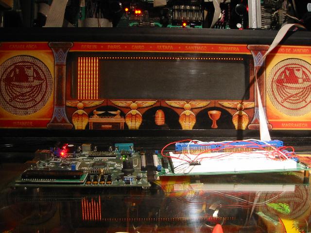
The test image shown on the DMD is produced by the Spartan development board.
The image is sharp with no ghosting showing that the timing is correct.
In the above image, the DMD data cable is plugged into a solderless breadboard that is in turn plugged into the Spartan board. I initially started to implement the circuit by simply converting the schematic from the WPC-89 schematics into VHDL. I soon realized that the discrete design was not very suitable for implementation in an FPGA. This is because good FPGA coding practices recommend a fully synchronous design. The original WPC-89 implementation is far from it. I rewrote the VHDL code as a fully synchronous design, and using only one clock (the CPU E-clock) rather than two as the original DMD interface board. By using a single clock, it makes it easier to one day integrate everything into one FPGA.
The DMD display shown working on a WPC-89 machine.
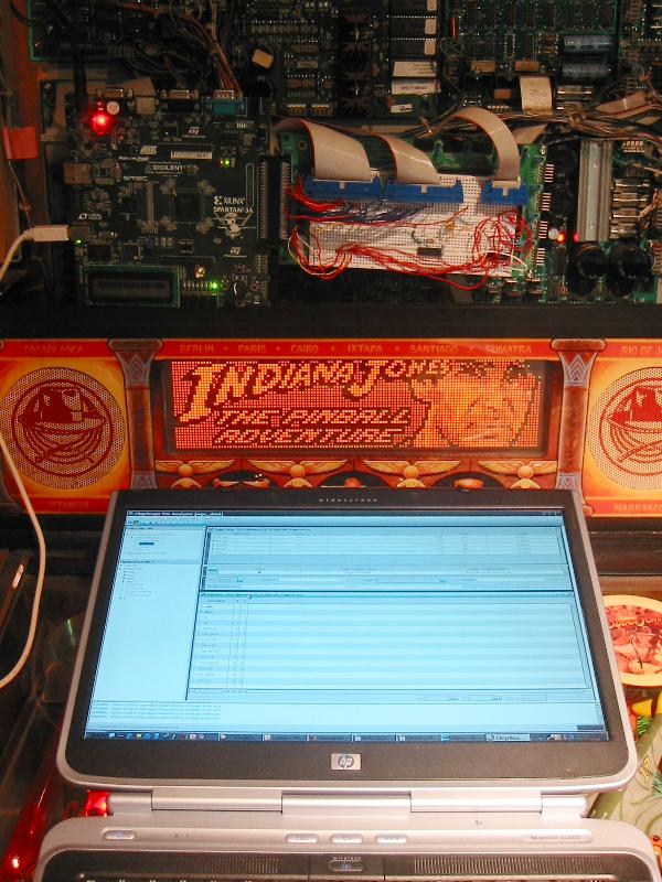
I develop the code on my laptop and load it into the FPGA via JTAG.
After another week's work, I found all the bugs and was able to drive the DMD by plugging into the CPUs IO expansion ribbon cables! It took more effort than I thought it would, and was mainly stymied by the design of the original controller. The way it switches the address bus into the RAM violated the FPGA RAM's hold time, and it took me a while to figure it out.
The photo above shows my development system. The solderless breadboard has the three connectors to the IJ (two to the CPU board, and one for the DMD). The Spartan board interfaces to these connectors, and is controlled by the CPU board. The laptop is simply set on the playfield glass, and connected via JTAG to the Spartan. I can then develop the code, and run it with Chipscope (on the laptop). This allows me access to the signals without a logic analyzer connected.
A day after I was able to successfully use the programmed Spartan on my Indiana Jones (WPC-89), I was able to use it on my Medieval Madness (WPC-95). This shows that the DMD interface on both generations are the same.
The CPU Board
In September 2007, after the successful completion of the WPC-95 A/V VHDL code, I started working on an FPGA version of the CPU board. Since so much of this board is digital in nature, it would lend itself well to recasting into an FPGA. After some searching, I found a 6809 core. If I could also combine the RAM and the ASIC's functionality, we would have the essential parts of the CPU board on a single FPGA. I also previously had the good fortune of purchasing a CPU board (with the valuable ASIC) on Ebay for $65. The board did not initially boot, but after I replaced the RAM, it booted fine. I was thus set to start the replication process.
I first loaded the game ROM code into the Flash memory that is on the Spartan board, and started by tackling the ROM paging that is done inside the ASIC. Information on how this is done is very sketchy, and even looking at the logic analyzer plots showed very little information. I then found this memory map by Matthias Bucher, and the PinMAME source code. Among the files in this latter resource, the file WPC.H contains the memory map locations of the ASIC registers, and a description of the "shifted bit hardware". I implemented my best guess of the paging algorithm, and it appeared to successfully step through the ROM check process (by using Chipscope).
With the logic analyzer hooked up to read the CPU's activity, I could roughly see what the WPC CPU does during the boot process:
